“ADC device tree configuration”的版本间的差异
Zhouyuebiao(讨论 | 贡献) (创建页面,内容为“== Article purpose == The purpose of this article is to explain how to configure the analog-to-digital converter (''ADC'')<ref name="ADC internal peripheral">ADC i…”) |
|||
| 第109行: | 第109行: | ||
<references /> | <references /> | ||
| − | |||
| − | |||
| − | |||
| − | |||
| − | |||
| − | |||
| − | |||
| − | |||
| − | |||
| − | |||
| − | |||
| − | |||
2020年11月9日 (一) 11:54的版本
目录
Article purpose
The purpose of this article is to explain how to configure the analog-to-digital converter (ADC)[1] when the peripheral is assigned to Linux® OS, and in particular:
- how to configure the ADC peripheral
- how to configure the board, e.g. the ADC voltage reference regulator, channels, pins and sampling time.
The configuration is performed using the device tree mechanism[2].
It is used by the ADC Linux driver that registers relevant information in IIO framework, such as IIO devices, channels and voltage scale for each ADC.
If the peripheral is assigned to another execution context, refer to How to assign an internal peripheral to a runtime context article for guidelines on peripheral assignment and configuration.
DT bindings documentation
STM32 ADC device tree bindings[3] describe all the required and optional functions.
DT configuration
This hardware description is a combination of STM32 microprocessor and board device tree files. See Device tree for more explanations on device tree file split.
The STM32CubeMX can be used to generate the board device tree. Refer to How to configure the DT using STM32CubeMX for more details.
DT configuration (STM32 level)
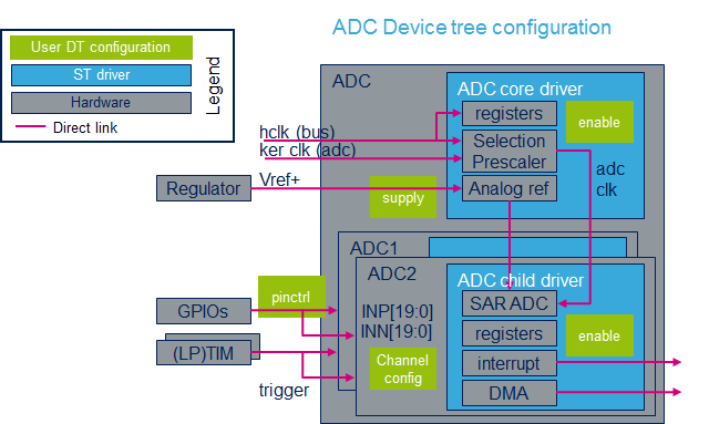
The ADC nodes are declared in stm32mp157c.dtsi[4].
- DT root node ('adc') describes the ADC hardware block parameters such as register areas, clocks and interrupts.
- DT child nodes ('adc1' and 'adc2') describe ADC1 and ADC2 independently.
adc: adc@address {
	compatible = "st,stm32mp1-adc-core";
	...                                      /* common resources in 'adc' root node. */
	adc1: adc@0 {
		compatible = "st,stm32mp1-adc";
		...                              /* private resources in 'adc1' child node. */
	};
	adc2: adc@100 {
		compatible = "st,stm32mp1-adc";
		...                              /* private resources in 'adc2' child node. */
	};
};
| This device tree part is related to STM32 microprocessors. It must be kept as is, without being modified by the end-user. |
DT configuration (board level)
Follow the sequences described in the below chapters to configure and enable the ADC on your board.
Common resources for all ADCs
The DT root node ('adc') must be filled in:
- Enable the ADC block by setting status = "okay".
- Configure the pins in use via pinctrl, through pinctrl-0 and pinctrl-names.
- Configure the analog supply voltage regulator[5] by setting vdda-supply = <&your_vdda_regulator>.
- Configure the analog reference voltage regulator[5] by setting vref-supply = <&your_vref_regulator>.
| The ADC can use the internal VREFBUF[6] or any other external regulator[5] wired to VREF+ pin. |
Resources dedicated to ADC1 and ADC2
The DT child nodes ('adc1' and/or 'adc2') must be filled in:
- Enable 'adc1' and/or 'adc2' by setting status = "okay".
- Enable single-ended channel(s) (<vinp...>) by setting st,adc-channels = <0 1 2...>.
- Enable differential channel(s) pairs (<vinp vinn>, ...) by setting st,adc-diff-channels = <1 0>, <2 6>, ....
- Set the minimum sampling time [7] for each or all channels by setting st,min-sample-time-nsecs = <10000> (optional).
- Set the resolution by setting assigned-resolution-bits = <12> (optional).
DT configuration example
The example below shows how to configure ADC1:
- Input pin: use Pinctrl device tree configuration to configure PF12 as analog input.
- Analog supply: it is provided by one of the PMIC LDO regulators.
- Voltage reference: it is provided by the VREFBUF internal regulator.
- Input channel: configure ADC1_IN6 (e.g on PF12).
- Sampling time: the minimum sampling time is 10 µs.
# part of pin-controller dt node
adc1_in6_pins_a: adc1-in6 {
	pins {
		pinmux = <STM32_PINMUX('F', 12, ANALOG)>; /* configure 'PF12' as ANALOG */
	};
};
&adc {
	/* ADC1 & ADC2 common resources */
	pinctrl-names = "default";
	pinctrl-0 = <&adc1_in6_pins_a>;              /* Use PF12 pin as ANALOG */
	vdda-supply = <&vdda>;                       /* Example to supply vdda pin by using a PMIC regulator
	vref-supply = <&vrefbuf>;                    /* Example to use VREFBUF (It needs to be enabled as well) */
	status = "okay";                             /* Enable ADC12 block */
	adc1: adc@0 {
		/* private resources for ADC1 */
		st,adc-channels = <6>;               /* ADC1 in6 channel is used */
		st,min-sample-time-nsecs = <10000>;  /* 10µs sampling time */
		status = "okay";                     /* Enable ADC1 */
	};
	adc2: adc@100 {
		/* private resources for ADC2 */
		...
	};
};
How to configure the DT using STM32CubeMX
The STM32CubeMX tool can be used to configure the STM32MPU device and get the corresponding platform configuration device tree files.
The STM32CubeMX may not support all the properties described in the above DT bindings documentation paragraph. If so, the tool inserts user sections in the generated device tree. These sections can then be edited to add some properties and they are preserved from one generation to another. Refer to STM32CubeMX user manual for further information.
References
For additional information, refer to the following links:
- ↑ ADC internal peripheral
- ↑ Device tree
- ↑ Documentation/devicetree/bindings/iio/adc/st,stm32-adc.txt | |}} Documentation/devicetree/bindings/iio/adc/st,stm32-adc.txt , STM32 ADC device tree bindings
- ↑ arch/arm/boot/dts/stm32mp157c.dtsi | |}} STM32MP157C device tree file
- ↑ 5.05.15.2 Regulator overview
- ↑ VREFBUF internal peripheral
- ↑ How to get the best ADC accuracy in STM32, by STMicroelectronics