“ADC device tree configuration”的版本间的差异
来自百问网嵌入式Linux wiki
| (未显示同一用户的6个中间版本) | |||
| 第31行: | 第31行: | ||
ADC节点在stm32mp157c.dtsi中声明<ref name="stm32mp157c_dtsi">{{CodeSource | Linux kernel | arch/arm/boot/dts/stm32mp157c.dtsi | STM32MP157C device tree file}}</ref>. | ADC节点在stm32mp157c.dtsi中声明<ref name="stm32mp157c_dtsi">{{CodeSource | Linux kernel | arch/arm/boot/dts/stm32mp157c.dtsi | STM32MP157C device tree file}}</ref>. | ||
| − | * ''' | + | *'''DT根节点'''(''''adc'''')描述ADC硬件模块参数,例如寄存器区域,时钟和中断。 |
| − | * ''' | + | * '''DT子节点'''(''''adc1''''和''''adc2'''')独立描述ADC1和ADC2。 |
adc: adc@address { | adc: adc@address { | ||
compatible = "st,stm32mp1-adc-core"; | compatible = "st,stm32mp1-adc-core"; | ||
| 第45行: | 第45行: | ||
}; | }; | ||
}; | }; | ||
| − | {{Warning| | + | {{Warning|该设备树部分与STM32微处理器有关。 它必须保持原样,而不能由最终用户修改。}} |
=== DT configuration (board level) === | === DT configuration (board level) === | ||
| − | + | 请按照以下章节中描述的顺序在板上配置和启用ADC。 | |
==== Common resources for all ADCs ==== | ==== Common resources for all ADCs ==== | ||
| − | + | 必须填写'''DT根节点'''(''''adc''''): | |
| − | * | + | * 通过设置'''status =“ okay”。'''来启用ADC模块。 |
| − | * | + | * 通过[[Pinctrl overview|pinctrl]],'''pinctrl-0'''和'''pinctrl-names'''配置正在使用的引脚。 |
| − | * | + | * 通过设置'''vdda-supply = <&your_vdda_regulator>'''来配置模拟电源稳压器<ref name="Regulator overview">[[Regulator overview]]</ref> 。 |
| − | + | * 通过设置'''vref-supply = <&your_vref_regulator>'''来配置模拟参考电压调节器<ref name="Regulator overview">[[Regulator overview]]</ref> 。 | |
| − | {{info| | + | {{info|ADC可以使用内部VREFBUF<ref name="VREFBUF internal peripheral">[[VREFBUF internal peripheral]]</ref> 或任何其他连接到VREF +引脚的外部稳压器<ref name="Regulator overview"/> 。}} |
==== Resources dedicated to ADC1 and ADC2==== | ==== Resources dedicated to ADC1 and ADC2==== | ||
| − | + | ''' DT子节点'''(''''adc1''''和/或''''adc2'''')必须填写: | |
| − | * | + | * 通过设置'''status =“ okay”。''来启用'adc1'和/或'adc2'。''' |
| − | * | + | * 通过设置'''st,adc-channels = <0 1 2 ...>。'''来启用单端通道(''<vinp ...>'') |
| − | + | * 通过设置'''st,adc-diff-channels = <1 0>,<2 6>,....'''来启用差分通道对(''<vinp vinn>,...'')。 | |
| − | * | + | * 设置最小采样时间 <ref>[http://www.st.com/content/ccc/resource/technical/document/application_note/group0/3f/4c/a4/82/bd/63/4e/92/CD00211314/files/CD00211314.pdf/jcr:content/translations/en.CD00211314.pdf How to get the best ADC accuracy in STM32], by STMicroelectronics</ref> 通过设置'''st,min-sample-time-nsecs = <10000>'''(可选)为每个或所有通道设置。 |
| − | * | + | * 通过设置'''assigned-resolution-bits = <12>'''(可选)来设置分辨率。 |
=== DT configuration example === | === DT configuration example === | ||
| − | + | 下面的示例显示如何配置ADC1: | |
| − | * | + | * 输入引脚:使用[[Pinctrl device tree configuration]]将PF12配置为模拟输入。 |
| − | * | + | * 模拟电源:由 [[PMIC hardware components|PMIC]] LDO稳压器之一提供。 |
| − | * | + | * 参考电压:由[[Regulator_overview#Microprocessor device internal regulators|VREFBUF internal regulator]]提供。 |
| − | * | + | * 输入通道:配置ADC1_IN6(例如在PF12上)。 |
| − | * | + | * 采样时间:最短采样时间为10 µs。 |
# part of pin-controller dt node | # part of pin-controller dt node | ||
| 第101行: | 第101行: | ||
==How to configure the DT using STM32CubeMX== | ==How to configure the DT using STM32CubeMX== | ||
| − | + | [[STM32CubeMX]] 工具可用于配置STM32MPU设备并获取相应的[[Device_tree#STM32|platform configuration device tree]]文件。<br /> | |
| − | + | STM32CubeMX可能不支持以上[[#DT bindings documentation|DT bindings documentation]] 段中描述的所有属性。 如果是这样,该工具会在生成的设备树中插入'''用户部分'''。 然后可以编辑这些部分以添加一些属性,并将它们一代一代地保留下来。有关更多信息,请参见[[STM32CubeMX]]用户手册。 | |
==References== | ==References== | ||
| − | + | 有关更多信息,请参考以下链接: | |
| − | |||
<references /> | <references /> | ||
2020年11月9日 (一) 14:50的最新版本
目录
Article purpose
本文的目的是解释在将外围设备分配给Linux® OS时如何配置模数转换器(“ ADC”)[1] :
- 如何配置ADC外围设备
- 如何配置board,例如 ADC参考电压调节器,通道,引脚和采样时间。
使用设备树机制执行配置[2].
ADC Linux driver 使用它在 IIO framework中注册相关信息,例如每个ADC的IIO设备,通道和电压标度。
如果外围设备已分配给另一个执行上下文,请参阅 How to assign an internal peripheral to a runtime context 文章,以获取有关外围设备分配和配置的准则。
DT bindings documentation
"STM32 ADC设备树绑定"[3] 描述所有必需和可选功能。
DT configuration
该硬件描述是STM32微处理器和电路板设备树文件的组合。 有关设备树文件分割的更多说明,请参见Device tree。 STM32CubeMX可用于生成板卡设备树。 有关更多详细信息,请参考 How to configure the DT using STM32CubeMX。
ADC DT configuration
DT configuration (STM32 level)
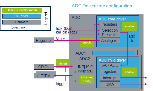
ADC节点在stm32mp157c.dtsi中声明[4].
- DT根节点('adc')描述ADC硬件模块参数,例如寄存器区域,时钟和中断。
- DT子节点('adc1'和'adc2')独立描述ADC1和ADC2。
adc: adc@address {
	compatible = "st,stm32mp1-adc-core";
	...                                      /* common resources in 'adc' root node. */
	adc1: adc@0 {
		compatible = "st,stm32mp1-adc";
		...                              /* private resources in 'adc1' child node. */
	};
	adc2: adc@100 {
		compatible = "st,stm32mp1-adc";
		...                              /* private resources in 'adc2' child node. */
	};
};
| 该设备树部分与STM32微处理器有关。 它必须保持原样,而不能由最终用户修改。 |
DT configuration (board level)
请按照以下章节中描述的顺序在板上配置和启用ADC。
Common resources for all ADCs
必须填写DT根节点('adc'):
- 通过设置status =“ okay”。来启用ADC模块。
- 通过pinctrl,pinctrl-0和pinctrl-names配置正在使用的引脚。
- 通过设置vdda-supply = <&your_vdda_regulator>来配置模拟电源稳压器[5] 。
- 通过设置vref-supply = <&your_vref_regulator>来配置模拟参考电压调节器[5] 。
| ADC可以使用内部VREFBUF[6] 或任何其他连接到VREF +引脚的外部稳压器[5] 。 |
Resources dedicated to ADC1 and ADC2
DT子节点('adc1'和/或'adc2')必须填写:
- 通过设置status =“ okay”。来启用'adc1'和/或'adc2'。
- 通过设置st,adc-channels = <0 1 2 ...>。来启用单端通道(<vinp ...>)
- 通过设置st,adc-diff-channels = <1 0>,<2 6>,....来启用差分通道对(<vinp vinn>,...)。
- 设置最小采样时间 [7] 通过设置st,min-sample-time-nsecs = <10000>(可选)为每个或所有通道设置。
- 通过设置assigned-resolution-bits = <12>(可选)来设置分辨率。
DT configuration example
下面的示例显示如何配置ADC1:
- 输入引脚:使用Pinctrl device tree configuration将PF12配置为模拟输入。
- 模拟电源:由 PMIC LDO稳压器之一提供。
- 参考电压:由VREFBUF internal regulator提供。
- 输入通道:配置ADC1_IN6(例如在PF12上)。
- 采样时间:最短采样时间为10 µs。
# part of pin-controller dt node
adc1_in6_pins_a: adc1-in6 {
	pins {
		pinmux = <STM32_PINMUX('F', 12, ANALOG)>; /* configure 'PF12' as ANALOG */
	};
};
&adc {
	/* ADC1 & ADC2 common resources */
	pinctrl-names = "default";
	pinctrl-0 = <&adc1_in6_pins_a>;              /* Use PF12 pin as ANALOG */
	vdda-supply = <&vdda>;                       /* Example to supply vdda pin by using a PMIC regulator
	vref-supply = <&vrefbuf>;                    /* Example to use VREFBUF (It needs to be enabled as well) */
	status = "okay";                             /* Enable ADC12 block */
	adc1: adc@0 {
		/* private resources for ADC1 */
		st,adc-channels = <6>;               /* ADC1 in6 channel is used */
		st,min-sample-time-nsecs = <10000>;  /* 10µs sampling time */
		status = "okay";                     /* Enable ADC1 */
	};
	adc2: adc@100 {
		/* private resources for ADC2 */
		...
	};
};
How to configure the DT using STM32CubeMX
STM32CubeMX 工具可用于配置STM32MPU设备并获取相应的platform configuration device tree文件。
STM32CubeMX可能不支持以上DT bindings documentation 段中描述的所有属性。 如果是这样,该工具会在生成的设备树中插入用户部分。 然后可以编辑这些部分以添加一些属性,并将它们一代一代地保留下来。有关更多信息,请参见STM32CubeMX用户手册。
References
有关更多信息,请参考以下链接:
- ↑ ADC internal peripheral
- ↑ Device tree
- ↑ Documentation/devicetree/bindings/iio/adc/st,stm32-adc.txt | |}} Documentation/devicetree/bindings/iio/adc/st,stm32-adc.txt , STM32 ADC device tree bindings
- ↑ arch/arm/boot/dts/stm32mp157c.dtsi | |}} STM32MP157C device tree file
- ↑ 5.05.15.2 Regulator overview
- ↑ VREFBUF internal peripheral
- ↑ How to get the best ADC accuracy in STM32, by STMicroelectronics